We predict that by operating a SiC MOSFET (exhibiting linear I-V characteristics) and an IGBT (exhibiting non-linear, quadratic-like I-V characteristics) in parallel with an optimal active area ratio, a next-generation power device with outstanding performance and cost efficiency across a wide operating range can be achieved. Furthermore, optimizing the gate drive timings of both chips can unlock unique benefits such as reduced switching losses. In this project, we validate the advantages of parallel configurations using device simulations, collaborating with external institutions for circuit-level simulations and empirical verification.

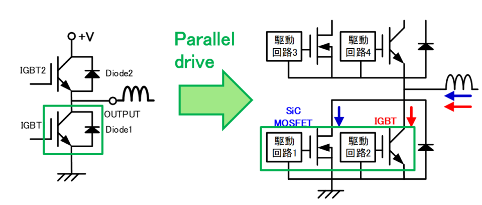
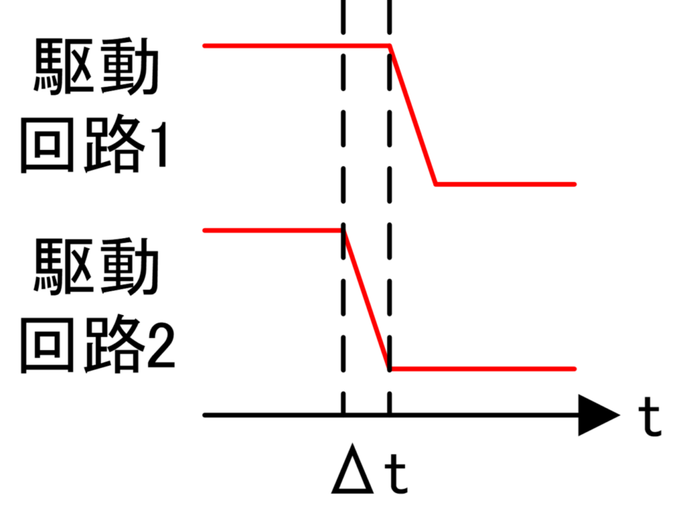
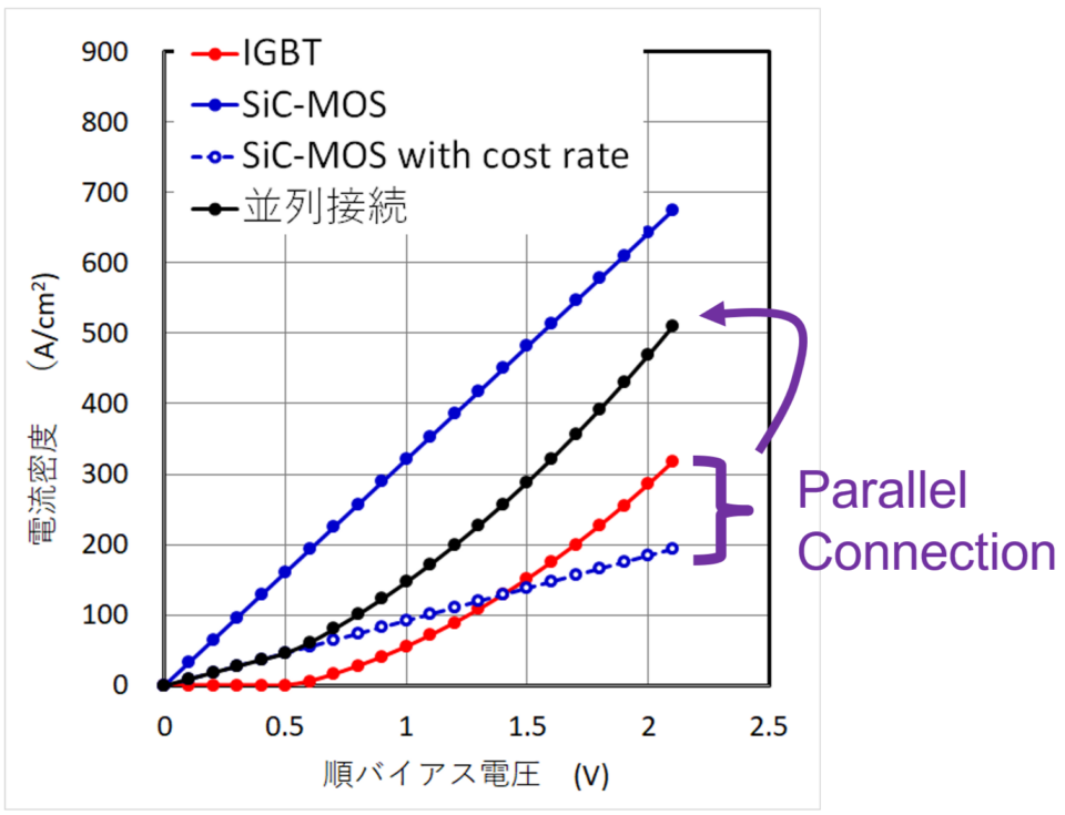
- Numerical validation via simulation
- Empirical demonstration through joint research projects