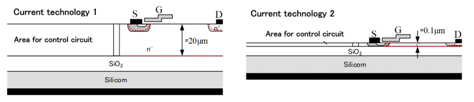
In system integration on Silicon-on-Insulator (SOI) wafers, research into embedding 600V-class high-voltage MOSFETs has been ongoing for over 30 years since the 1990s. However, conventional techniques required thickening the active layer, which raised manufacturing costs and introduced severe fabrication barriers due to “wafer warpage.” Our laboratory has proposed several proprietary innovations to overcome these long-standing bottlenecks. Currently, we are conducting device physics verification via TCAD simulation, striving for a major breakthrough to disrupt three decades of technological stagnation.

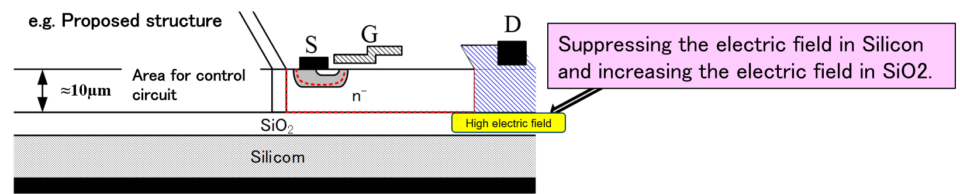
- Proposals of unique proprietary technological innovations
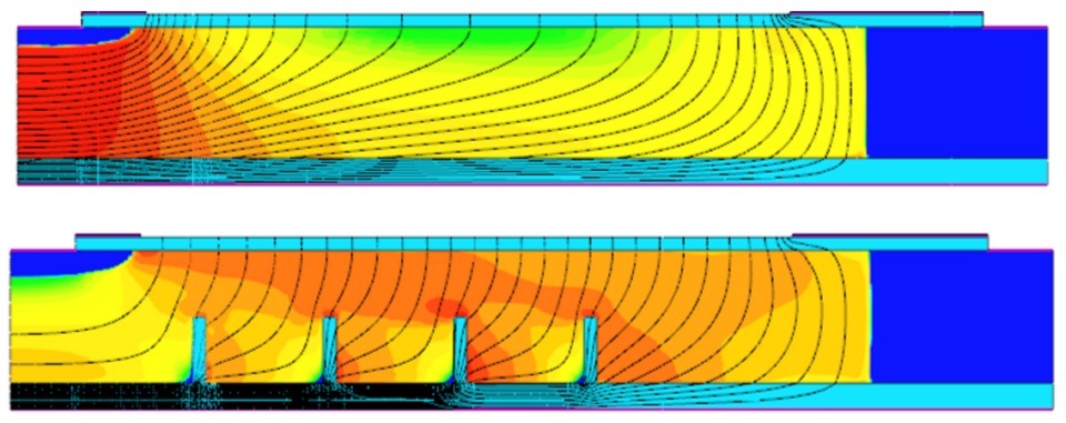
- Device operation and physics validation using TCAD numerical simulation